To reduce the chamber-to-chamber variation and to optimize the yield of an etching tool, HORIBA offers a wide range of fluid control modules and smart sensors for endpoint detection and chamber health monitoring. Compact and robust, they can be used for R&D and for Production.
Dry etching refers to the removal of material, typically a masked pattern of semiconductor material, by exposing the material to a bombardment of ions (usually a plasma of reactive gases such as fluorocarbons, oxygen, chlorine, boron trichloride; sometimes with addition of nitrogen, argon, helium and other gases) that dislodge portions of the material from the exposed surface. A common type of dry etching is reactive-ion etching. Unlike with many (but not all, see isotropic etching) of the wet chemical etchants used in wet etching, the dry etching process typically etches directionally or anisotropically.
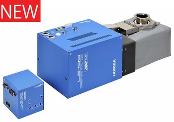
Wafer Back Side Cooling System
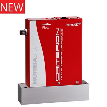
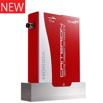
High Speed & Precision Pressure Insensitive Mass Flow Module
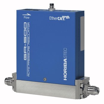
Wide Range Pressure Insensitive Mass Flow Module

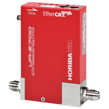
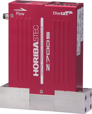
Pressure Insensitive Mass Flow Module
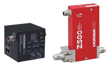
Ultra-thin Mass Flow Controller
Thermal Flow Splitter
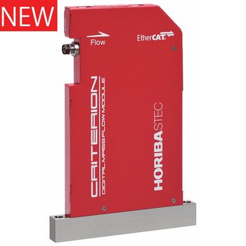
New concept Pressure Insensitive Mass Flow Module

Digital Liquid Mass Flow Meters
HORIBA's expertise in analytical instrumentation has provided the foundations for a range of successful industrial monitoring tools for the semiconductor, pharmaceutical and chemical industries.
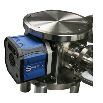
With its new compact design and enhanced image quality, the LEM interferometer for in-situ etch rate monitoring and end-point detection can be mounted on any process chamber with a direct top view of the wafer. It provides a real-time digital CCD image of the sample surface, making its 30-m laser beam positioning simple and accurate. Based on interferometry technique, the LEM provide in-situ etch/growth rate monitoring for endpoint detection of a wide range of dry etch applications.
Laser Gas Analyzer
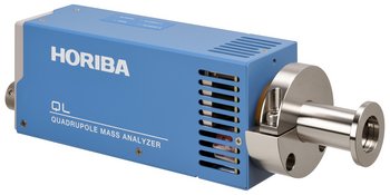
Quadrupole Mass Analyzer
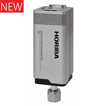
Capacitance Manometer

X선 분석 현미경 초대형 챔버 모델

Optical Emission Spectroscopy Etching End-point Monitor
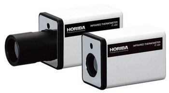
High-Accuracy Infrared Thermometers [Stationary type]

Camera Endpoint Monitor based on Real Time Laser Interferometry

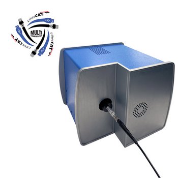
Miniature Multi Communication UV-NIR Spectrometer
UV-VIS-NIR Spectrometer
Multispectra, Multifiber, Multichannel Imaging spectrometer with 8-16-32 Simultaneous UV-NIR Spectra
Most Compact Vacuum UV Back-Illuminated CCD Spectrometer (VUV-FUV)
HORIBA제품의 자세한 정보를 원하시면, 아래의 양식에 내용을 입력을 부탁드립니다.