<< Back to OEM Solutions for your Applications
In the fast-evolving world of semiconductor fabrication, maintaining accuracy, consistency, and efficiency is crucial to achieving high yields and reliable device performance. HORIBA provides advanced process control and metrology solutions that help manufacturers optimize critical steps, prevent defects, and ensure the highest quality standards.
From real-time monitoring of plasma etching and deposition processes, to high-precision measurements of wafer structures, HORIBA’s Optical Emission Spectroscopy (OES), hyperspectral imaging, and Raman spectroscopy, enable manufacturers to achieve stable, repeatable, and high-performance semiconductor production. Explore our solutions to see how we support innovation in semiconductor manufacturing.
Process control in semiconductor manufacturing ensures the accuracy, consistency, and efficiency of critical fabrication steps, such as plasma etching, deposition, and chamber cleaning. It is essential for maintaining high yield, preventing defects, and ensuring the reliability of advanced semiconductor devices.
Effective process control involves continuous monitoring of key parameters, rapid detection of deviations, and real-time adjustments to maintain optimal performance. Inadequate control can result in variations in plasma conditions or deposition quality, potentially leading to device failure and reduced operational efficiency.
To address these challenges, advanced diagnostic technologies like Optical Emission Spectroscopy (OES), (multiwavelength) interferometry and hyperspectral imaging—provide real-time insights into process dynamics. These tools enable precise endpoint detection, uniformity control, and contamination prevention, thereby supporting stable and repeatable manufacturing processes.
Metrology in semiconductor manufacturing ensures precision, quality control, and process optimization by enabling accurate measurements of wafers, thin films, and device structures. It is essential for detecting defects, maintaining uniformity, and ensuring high performance in advanced semiconductor devices.
This process involves techniques like reflectometry for layer thickness analysis, multitrack spectroscopy and hyperspectral imaging for wafer mapping, and Raman spectroscopy for material characterization. These methods provide critical insights into structural and compositional properties at the nanoscale.
HORIBA’s cutting-edge metrology solutions empower semiconductor manufacturers with high-precision measurements, ensuring process reliability, yield improvement, and compliance with the stringent demands of modern semiconductor fabrication.
Procedente igitur mox tempore cum adventicium nihil inveniretur, relicta ora maritima in Lycaoniam adnexam Isauriae se contulerunt ibique densis intersaepientes itinera praetenturis provincialium et viatorum opibus pascebantur.

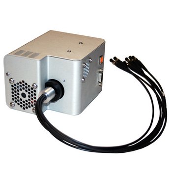
基于光发射光谱和 MWL 干涉测量法的工艺终点/反应腔健康监测

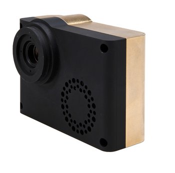
高光谱速率和高动态范围微型光谱仪

基于实时激光干涉测量的摄像头终点监测
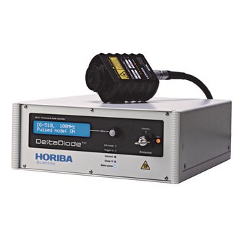
脉冲激光器和 LED 光源
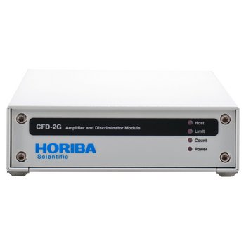
放大器-鉴频器
detector technology HORIBA在TCSPC检测器技术的全新发展
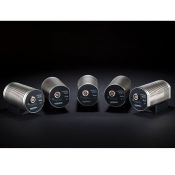
具有皮秒级精度的单光子检测器
如您有任何疑问,请在此留下详细需求信息,我们将竭诚为您服务。