MiPLATO-SiC

SiC Wafer Defect Inspection System

The SiC Wafer Defect Inspection System MiPLATO-SiC is a PL mapping system optimized for SiC wafers.
It acquires the spectrum of the entire wafer in a short time using spiral mapping, enabling simultaneous measurement of defect density, carrier lifetime, and film thickness variation. The deep-learning function performs automatic defect classification, enabling advanced defect type identification and assessment. The Auto Navigation function during spectrum mapping allows defect location identification and automatic tracking using PL map coordinates, DIC images, stage coordinates, etc. This system is capable of detecting and analyzing fine defects on wafers.

Segment: Semiconductor
Division: Metrology

General Features

• Simultaneous measurement of 3-channel photoluminescence and 1-channel DIC laser microscopy using a 355nm laser source
• Deep learning for defect analysis
• DIC Laser Microscopy Surface Inspection
  – Reflected DIC laser microscope of excitation source (355nm)
  – Carrot, Scratch, Droplets, 3-C triangular defects
• Band edge PL inspection method, additional 2 types of data for user reference
  – BPD, Shockley stacking faults, Bar type stacking faults
• Photoluminescence spectral mapping with spectrometer
  – Whole wafer mapping
  – Spectroscopic analysis for aimed area in map data
• Auto-Navigation Function
  – Auto-defect inspection using spectral measurement using PMT mapping and image processing result
  – Exact stacking faults classification by spectrum analysis


Optical Configuration

• Spiral scan with 1800 RPM (Max) rotation stage
  – One head type & Two head type (under development)
• Micro PL with 50x objective lens
  – 2um beam size
• Multi detectors :
  – Default : reflected DIC, Band – edge PL, Spectrometer
Two additional customer designed PL defectors


Spectrum mapping (Macro)

• Macro mapping for substrate & Epi-wafer can be used for QC
  – Growth machine to machine
  – Ingot to ingot
  – Wafer to wafer in ingot
  – Wafer uniformity
     > 5 mins/ 6” with 3mm step


Spectrum mapping (Micro)


Auto-Navigation function

• screen capture image of spectrum acquisition process
   1. Mapping Image by PMT
   2. Cropped Imgae of SF being measured
   3. Spectrum ddata of SF
   4. Detailed information of SF from spectrum
   5. Report of Classified SFs


Mapping Result

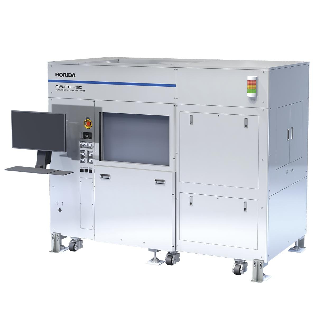
General Specification.​

Scan methodSpiral scan with 1800 RPM rotation and linear motion
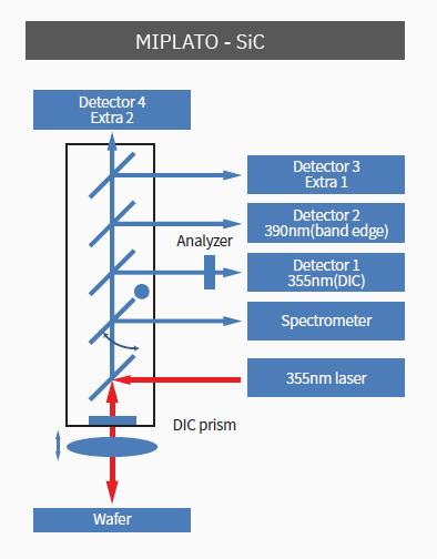
Laser20mW 355nm CW Laser
* Beam size on surface : 2um diameter thru 50x objective lens
Detector4 PMTs, 1 Spectrometer
StageXY-axis Linear stage
R stage with 1800RPM (Max)
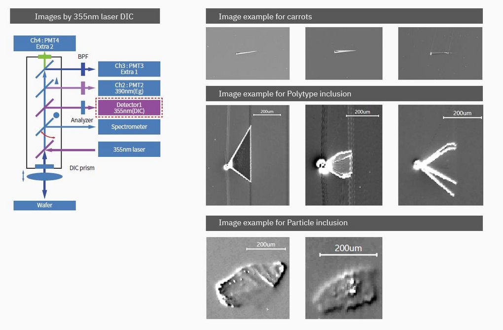
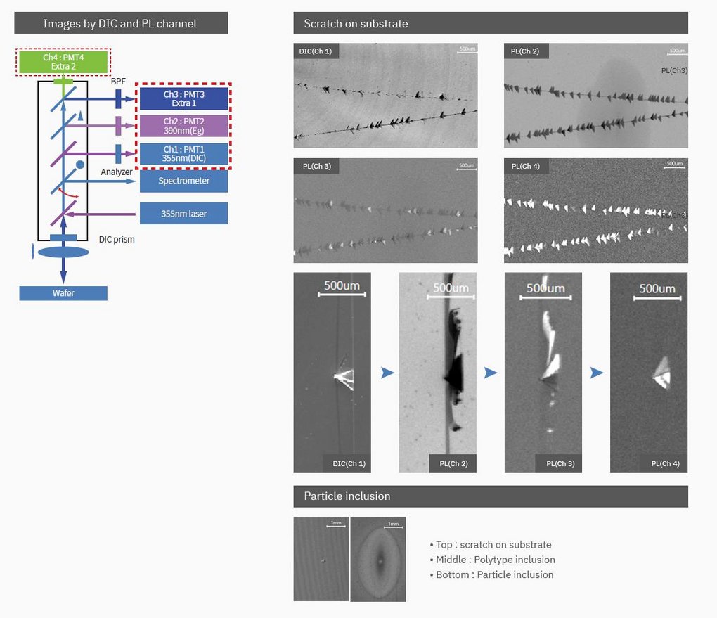
MeasurementPMT1DIC 355 Laser line for surface inspection
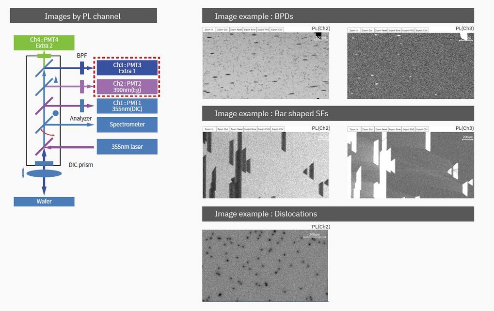
PMT 2,3,4PL Port 2 (PMT 2) : PL Inspection with 390nm bandpass filter
PL Port 3 (PMT 3) : 420 nm ~ 500 nm default.
But customer choose bandpass filter between these range
PL Port 4 (PMT 4) : 3C triangular defects with 540 nm bandpass
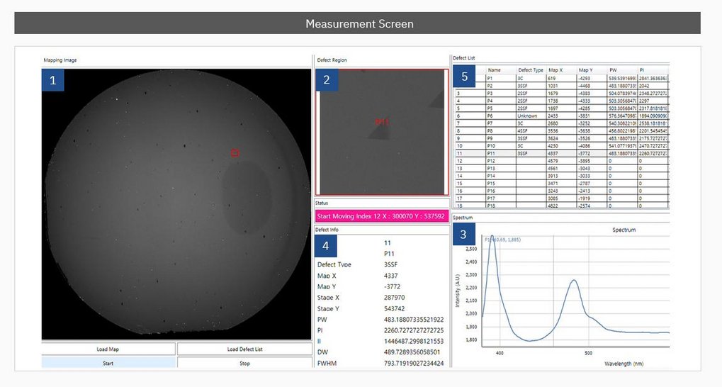
CCD cameraImage of designated position in analysis process
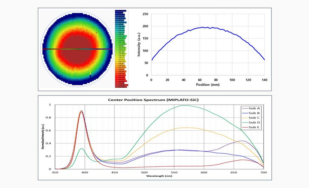
SpectrometerSpectrum between 380 nm ~ 700 nm
Detailed defects analysis, Macroscopic wafer deep level mapping
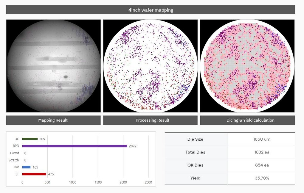
Measurement speed  4inch6inch
PMT Mapping
(4 channel at same time,
5um step)
8pcs / 1H6pcs / 1H
16pcs / 2H12 pcs / 2H
Spectrometer mapping
3mm step
 5 min
Dimension (mm) 2000 (w) x 1400 (d) x 2000 (h)

Utility.

Operating
Environment
PlaceClean Room (class ~ 10000)
Temperature15 ~ 35° C
Humidity< 85 % RH with no condensation
UtilityDimensions1500 mm x 2000 mm x 2300 mm, incl. HEPA filter
Weight1760 kg
Input Voltage220V± 10% 50 / 60Hz single phase
Full load current47A
Vacuum140L / min, -80KPa
Pipe size : Outer diameter 6mm
Vacuum2120L / min, -40KPa
Pipe size : Outer diameter 6mm
Air90L / min, 0.5MPa
Pipe size : Outer diameter 6mm

Solicitud de Información

Tiene alguna pregunta o solicitud? Utilice este formulario para ponerse en contacto con nuestros especialistas.

* Estos campos son obligatorios.