
原子力显微镜-拉曼系统结合了原子力显微镜(AFM)与光谱技术,可同步获取共定位的物理与化学数据。通过采用等离子金属镀层 AFM 探针,两种数据均可实现纳米级空间分辨率采集,特别适合新兴二维半导体材料和器件的表征研究。通过获取以下关联信息可实现全面分析:
|
|
十五年来,HORIBA 始终提供经 TERS 验证的系统解决方案,通过将原子力显微镜模式与光学光谱技术完美整合,配备最人性化的稳健技术平台,助力最先进半导体材料的研发应用。
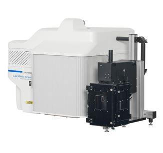 | 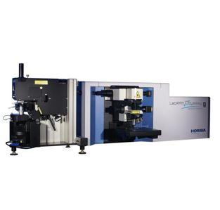 | ||
| LabRAM Soleil Nano | LabRAM Odyssey Nano | ||
| 用户人体工学设计 | 物镜压电调节,确保探头/光谱激光稳健精确对准 | ||
| 波长范围 | 300-1600 nm | 200 nm-2200 nm | |
| 标准波数截止值 | < 30cm-1 | < 50cm-1 | |
| 激光器 | 最多可内置 4 个全自动电机驱动并由计算机控制 | 最多 6 个全自动电机驱动 | |
如您有任何疑问,请在此留下详细需求信息,我们将竭诚为您服务。