







PDF
3.92
MB

Application Overview
Semiconductor : Mask / Lithography Process

Lithography process involves transferring the circuit patterns from a photomask onto a wafer using extreme ultraviolet (EUV) or deep ultraviolet (DUV) light. If there are contaminants on the photomask, this can lead to defects in the transferred circuit pattern, significantly impacting yield. From the photomask manufacturing process to semiconductor lithography, HORIBA provides products that help improve yield through particle control and the evaluation of pellicles and photoresists properties.
The PD Xpadion (PD10) Reticle/ Mask Particle Detection System uses laser scattering technology and image processing to inspect reticles and masks for particles. Equipped with auto-focus and image capture functions, it is easy to operate and supports process control in semiconductor manufacturing lines and photomask fabrication facilities. Additionally, the PD Xpadion (PD10-EX), based on the PD10, incorporates a particle removal function, enabling a complete process from detection to removal with a single unit. Furthermore, HORIBA has developed an in-house automated transport systems for reticles and masks, helping to the streamlining of semiconductor manufacturing processes and improved yield.
The RP-1 Reticle/Mask Particle Remover removes contaminants from reticle and mask surfaces. Using specialized probes positioned above and below the sample, it simultaneously dislodges contaminants and captures them by vacuum suction, preventing them from dispersing and re-adhering. Routine particle removal helps keep production lines clean and contributes to lower operating costs by extending the interval between mask cleaning cycles. When combined with the PD10, particle removal and particle inspection can be performed in a single sequence (PD10-EX).
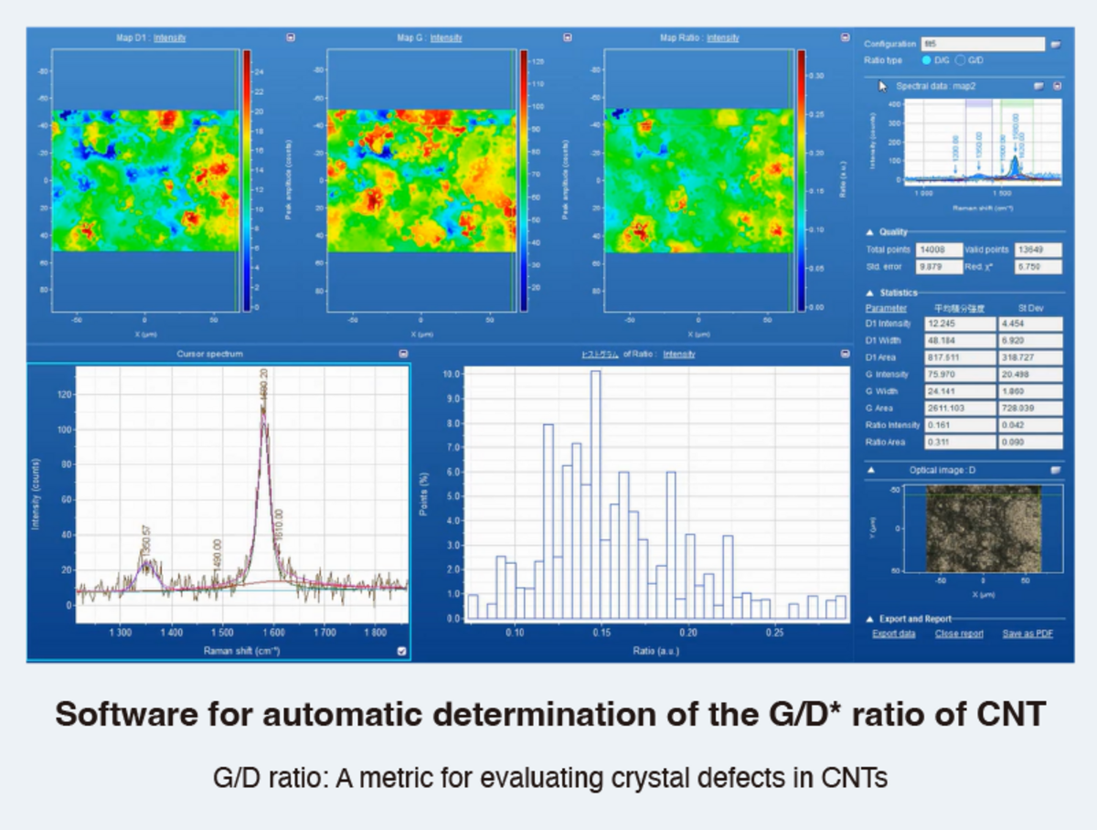
Raman spectroscopy is well-suited for characterizing carbon nanotube (CNT) pellicles under consideration for use in EUV processes. The XploRA PLUS Raman Microscope can evaluate and analyze CNT pellicle wear and lifetime, supporting process and quality control.
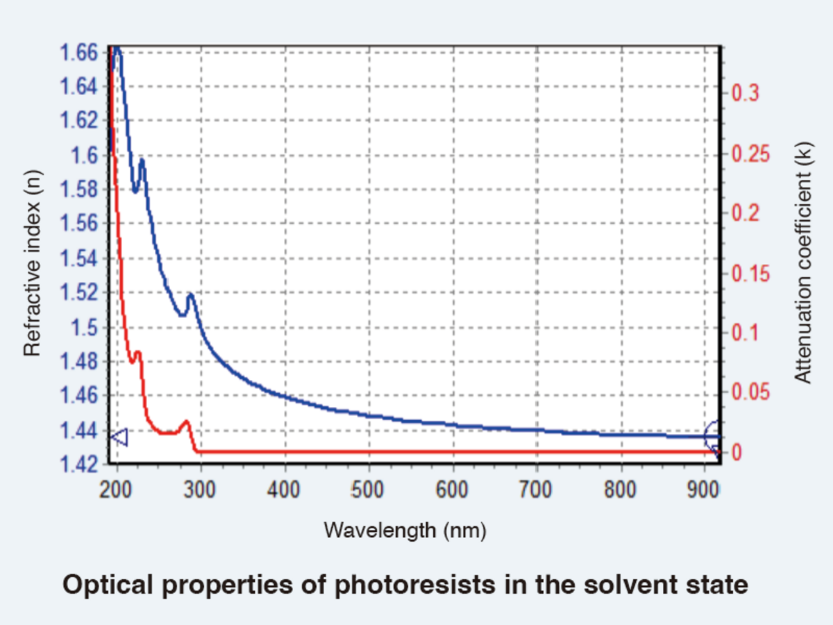
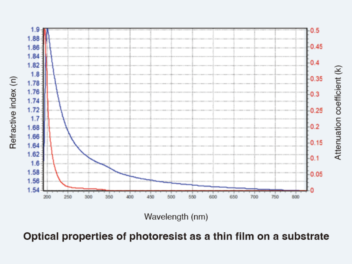
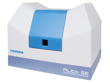
Quality control for the various photoresists used in the lithography process relies heavily on characterization of their optical properties and the control of film thickness after coating. The Auto SE Spectroscopic Ellipsometer for Simple Thin Film Measurement uses spectroscopic ellipsometry to measure and map the optical properties and film thickness of photoresists on wafers at the micro-scale, supporting quality control from material development to semiconductor production lines.
如您有任何疑问,请在此留下详细需求信息,我们将竭诚为您服务。