
光致发光光谱(PL)是一种用于表征半导体材料的重要光学方法。其原理是通过光源照射样本:当材料吸收光能后会产生电子-空穴对——价带中的电子跃迁至导带并留下空穴。复合过程中发射的光子能量对应于价带与导带之间的能量差,因此其能量低于激发光子。光致发光技术可用于检测:
|
|
HORIBA 是光学光谱领域的全球领导者,拥有超过 50 年的技术创新优势。光致发光特性分析技术能够为半导体材料(如 IV 族半导体、化合物半导体、二维材料)及其器件提供有价值的性能洞察。
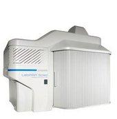 | 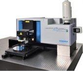 | 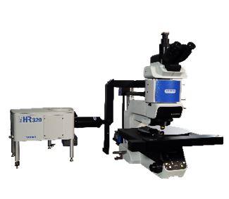 | |
| LabRAM Soleil | LabRAM Odyssey Semiconductor | SMS | |
| 波长范围 | 300-1600 nm | 200 nm-2200 nm | 250 – 14000 nm |
| 激光器 | 最多可内置 4 个全自动电机驱动并由计算机控制 | 最多 6 个全自动电机驱动 | 最多可支持 3 个样品,半电动式 |
| 可容纳样品尺寸 | 8” | 12” | 12” |
| 检测器 | 开放式电极 CCD,可选配 EMCCD,可选配 InGaAs 阵列探测器(最多 2 个探测器)。 | 开放式电极 CCD,光学 EMCCD,光学 InGaAs 阵列探测器(最多 3 个探测器)。 | CCD、IGA 及单通道 |
如您有任何疑问,请在此留下详细需求信息,我们将竭诚为您服务。