
拉曼光谱是一种非破坏性化学分析技术,通过光的非弹性散射研究样品的振动模式。该技术可为半导体行业提供优化研发流程和提高器件良率的详细信息:
|
|
HORIBA 是全球拉曼光谱技术的领导者,拥有超过 50 年的技术创新积淀。利用拉曼表征技术,可深入解析 IV 族半导体、化合物半导体、二维材料及其器件等半导体材料的特性。
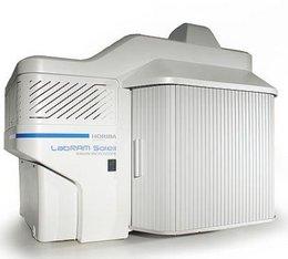 | 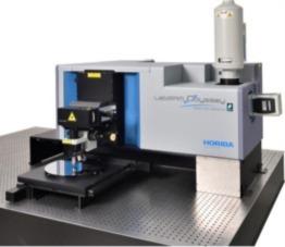 | |
| LabRAM Soleil | LabRAM Odyssey Semiconductor | |
| 波长范围 | 300-1600 nm | 200 nm-2200 nm |
| 电动载物台 | 75 mm x 50 mm 或 120 mm x 80 mm | 300 mm x 300 mm |
| 激光器 | 最多配置 4 个全电机驱动且计算机控制的内置单元 | 最多 6 个全自动电机驱动 |
| 光谱分辨率(使用 1800 gr/mm 光栅的785 nm激发波长) | ≤ 0.9 cm-1 | ≤ 0.2 cm-1 |
| 光谱稳定性均方根值(基于硅 520 cm -1 谱线测量) | < 0.02 cm-1 | < 0.02 cm-1 |
如您有任何疑问,请在此留下详细需求信息,我们将竭诚为您服务。