
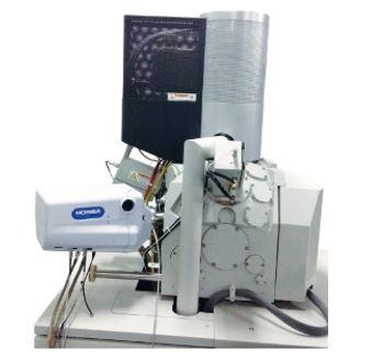
陰極發光 (CL) 是一種無損技術,基於高能量電子束(或「陰極射線」)激發下材料發出的光。安裝在 SEM 顯微鏡中的 CL 檢測器可用作表徵生長和裝置製程開發和探測中的半導體材料的強大工具:
|
|
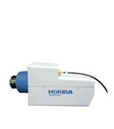
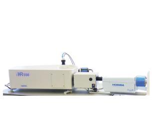
HORIBA offers CL one port-interface solutions that are compatible with all commercial SEM and FIB systems. With its wide emission energy ranging from 0.5 to 6 eV, its Raman capability, and its spatial resolution ranging from µ to nano, the Horiba CLUE systems can analyze a broad panel of semiconducting materials: group IV, II-VI, III-Vs, III-nitrides, wide band gap (SiC), 2D materials, Quantum dots, Nanowires as well as devices for optoelectronics, photovoltaics, LEDs.
 |  |  | |
| F-CLUE | H-CLUE | R-CLUE | |
| Coupling | Fiber | Direct | Fiber |
| Compatibility | All SEMs | All SEMs | All SEMs |
| Collection | Motorized Paraboloid mirror with fully retractable mechanism | ||
| Automation | Fully automated | ||
| Signal collection | ImagingCL, Spectral & Hyperspectral CL, Time-resolved CL | Imaging CL, Spectral & Hyperspectral CL, Time-resolved CL, Angular-resolved CL | Raman, PL, CL |
如您有任何疑問,请在此留下詳細需求或問題,我們將竭誠您服務。