
AFM-拉曼系統結合了原子力顯微鏡 (AFM) 和光譜學,可提供共定位的物理和化學數據。透過使用等離激元金屬塗層 AFM 探針,可以以奈米級空間分辨率收集這兩種數據,最適合新興 2D 半導體材料和裝置的表徵。透過以下相關資訊可以進行全面分析:
|
|
15 年來,HORIBA 為經過 TERS 驗證的系統提供了介面最簡單且最強大的技術,將 AFM 模式與光學光譜相結合,以部署最先進的半導體材料。
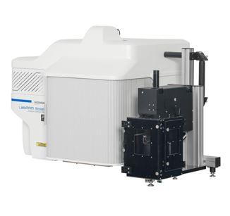 | 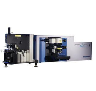 | ||
| LabRAM Soleil Nano | LabRAM Odyssey Nano | ||
| User Ergonomy | Piezo adjustment of objective for robust and accurate probe/spectroscopy laser alignment | ||
| Wavelength range | 300-1600 nm | 200 nm-2200 nm | |
| Standard wavenumber cut-off | < 30cm-1 | < 50cm-1 | |
| Lasers | Up to 4 built in fully motorized and computer controlled | Up to 6 fully motorized | |
如您有任何疑問,请在此留下詳細需求或問題,我們將竭誠您服務。