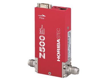
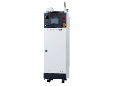
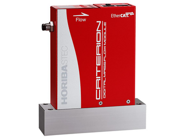
Deposition process is a key step in the semiconductor industry. HORIBA offers a wide range of products to optimize this process and to increase the yield
Atomic layer deposition (ALD) is a thin-film deposition technique based on the sequential use of a gas phase chemical process. ALD is considered a subclass of chemical vapour deposition. The majority of ALD reactions use two chemicals, typically called precursors. These precursors react with the surface of a material one at a time in a sequential, self-limiting, manner. Through the repeated exposure to separate precursors, a thin film is slowly deposited. ALD is a key process in the fabrication of semiconductor devices, and part of the set of tools available for the synthesis of nano materials.
Plasma-Enhanced ALD is a technique where plasma is used to enhance an atomic layer deposition (ALD) process, forming a thin-film coating. Like standard ALD, PEALD reacts specific chemical precursors but also cycles an RF-plasma to better control chemical reactions within the process. This allows high levels of conformality in production. It also requires a much lower temperature than standard ALD, making it suitable for temperature-sensitive materials.
Chemical vapor deposition (CVD) is a deposition method used to produce high quality, high-performance, solid materials, typically under vacuum. The process is often used in the manufacture of semiconductors and in the production of thin films.
In typical CVD, the substrate is exposed to one or more volatile precursors, which react and/or decompose on the substrate surface to produce the desired deposit. CVD has an extended family of processes which build upon the primary principles of CVD most commonly these are:
Atmospheric pressure CVD (APCVD) / Low-pressure CVD (LPCVD)
Ultrahigh vacuum CVD (UHVCVD)
Plasma-Enhanced CVD (PECVD)
Atomic-layer Deposition.
Metalorganic chemical vapor deposition (MOCVD)
Physical vapor deposition (PVD) describes a variety of vacuum deposition methods which can be used to produce thin films and coatings. PVD is characterized by a process in which the material goes from a condensed phase to a vapor phase and then back to a thin film condensed phase. The most common PVD processes are sputtering and evaporation. PVD is used in the manufacture of items which require thin films for mechanical, optical, chemical or electronic functions.
Sputtering techniques include; Magnetron, Ion Beam, Reactive, Ion Assisted, Gas Flow.
Evaporation involves two basic processes: a hot source material evaporates and condenses on the substrate.
高速精密壓力式質量流量模組
寬範圍壓力式質量流量模組
Mass Flow Controller
Digital Mass Flow Controller
Pressure Insensitive Mass Flow Module
超薄型質量流量模組
Multi Range/Multi Gas Digital Mass Flow Controller
新型壓力不敏感質量流量模組
熱感式分流器
Piezo Actuator Valve
Digital Automatic Pressure Regulator
Mixed Injection System Liquid Vaporizer
Direct Liquid Injection System
Compact Baking System
大流量液源汽化控制系統
Mixed Injection System Liquid Vaporizers
Digital Liquid Mass Flow Meters / Controllers
Liquid Auto Refill System
Quadrupole Mass Analyzer
Capacitance Manometer
Vapor Concentration Monitor
High-grade type Gas Monitor for Chamber Cleaning End Point Monitoring
Plasma Emission Controller
High-Accuracy Infrared Thermometer [Built-in type]
高精度紅外線測溫儀【內建型】
高精度紅外線測溫儀【固定式】
發射光譜和MWL測量的終端與腔室健康監測
Optical Emission Spectroscopy Etching End-point Monitor
UV-VIS-NIR Spectrometer
Multispectra, Multifiber, Multichannel Imaging spectrometer with 8-16-32 Simultaneous UV-NIR Spectra
Most Compact Vacuum UV Back-Illuminated CCD Spectrometer (VUV-FUV)
Miniature Multi Communication UV-NIR Spectrometer
即時雷射測量監控系統
Software Information
Open Source Software
EtherCAT Communication
如您有任何疑問,请在此留下詳細需求或問題,我們將竭誠您服務。