
光致發光光譜(PL)是一種用於表徵半導體材料的強大光學方法。 PL 是根據在樣品上照射光:吸收光後創造電子-電洞對:電子從價帶躍遷到導帶,留下電洞。複合時發射的光子對應於價帶和導帶之間的能量差,因此能量低於激發光子。 PL 可用於尋找:
|
|
HORIBA Scientific 是光譜學領域的世界領導者,擁有 50 多年的技術創新優勢。 PL 表徵可讓您深入了解半導體材料的特性,例如 IV 族半導體、化合物半導體、2D 材料及其裝置。
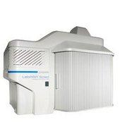 | 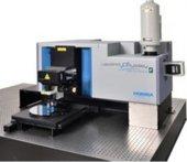 | 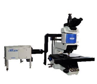 | |
| LabRAM Soleil | LabRAM Odyssey Semiconductor | SMS | |
| Wavelength range | 300-1600 nm | 200 nm-2200 nm | 250 – 14000 nm |
| Lasers | Up to 4 built in fully motorized and computer controlled | Up to 6 fully motorized | Up to 3, semi-motorized |
| Sample size acceptance | 8” | 12” | 12” |
| Detector | Open Electrode CCD, optional EMCCD, optional InGaAs arrays detector (max. 2 detectors). | Open Electrode CCD, optical EMCCD, optical inGaAs arrays detector (max. 3 detectoers). | CCD, IGA and sigle channel |
如您有任何疑問,请在此留下詳細需求或問題,我們將竭誠您服務。