
AFM 是一種無損掃描技術,使用末端帶有鋒利尖端的懸臂掃描樣品表面。 AFM 是半導體製造製程步驟奈米級表徵的首選工具。 AFM 提供不同的模式來提供:
|
|
HORIBA 提供第一個 100% 自動化系統(AIST 技術),可用於研究傳統以及最先進的半導體材料的形貌、電氣和機械特性。其設計經過專門開發,能夠與光學光譜(SNOM、拉曼、光致發光和 TERS/SERS 技術)無縫整合。
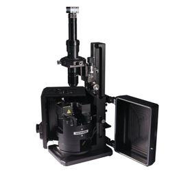 SmartSPM | |
| Automated Adjustment | Fully motorized and software-controlled laser / cantilever and photodiode alignment. |
| Optical access for upgradeability | Possible coupling to optical spectroscopies (PL & Raman) |
| Sample scanning range | 100 µm x 100 µm x 15 µm (±10 %) |
| Noise |
|
如您有任何疑問,请在此留下詳細需求或問題,我們將竭誠您服務。