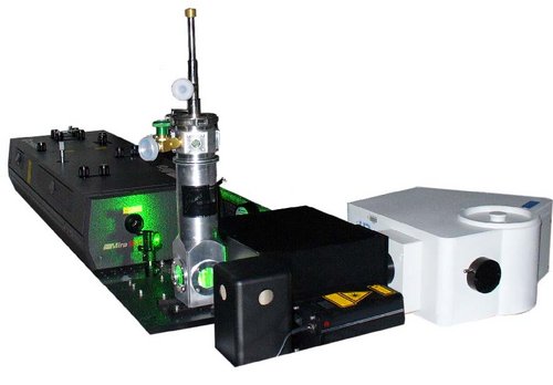
Raman and Resonance Raman Spectroscopy of Enzymes

The TRIAX and iHR series spectrometers used in Raman system configurations provide superior imaging performance with no re-diffracted light and maximized optical throughput.
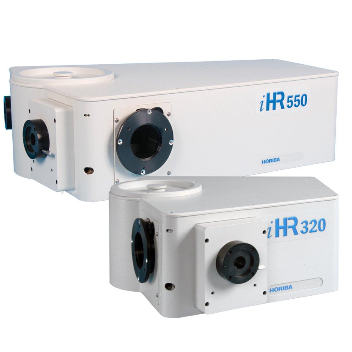
イメージングスペクトロメータ iHR320/iHR550
ユニークなデザインの、ユニークな分光器です。通常のCzerny-Turnerマウントの分光器のような、角型の分光器と異なるデザインは、きわめて高品位なイメージング性能を得るために、また、高いスループットを得るために採用されました。計算された光学設計により、CCD検出器を使用した場合、イメージングもしくはレゾリューションで最適化できます。数多くのアプリケーションに対応した、使いやすく、信頼性の高い中型分光器です。
| 焦点距離 | 320mm |
|---|---|
| 開口比 | f/4.1 |
| グレーティングマウント | 1枚〜3枚(交換可能) |
| グレーティングサイズ | 68mm × 68mm |
| 駆動範囲 | 150〜1500nm |
| フォーカルプレーン | 30mm wide × 12mm high |
| 逆線分散 | 2.31nm/mm at 500nm |
| 分解能 | 0.06nm(スリット、PMT使用時) |
| 波長精度 | ±0.2nm |
| 波長再現性 | ±0.075nm |
| 駆動最小ステップ | 0.002nm |
| 駆動速度 | 160nm/S |
| ストレーライト | 1.5x10⁻⁴ |
| インターフェース | USB2.0 |
| スリット | 電動0〜2mm(0〜7mmオプション) |
| 大きさ WxDxH | 422×417×192mm |
| 光軸高さ | 98mm |
| 重さ | 20.0Kg |
1200gr/mmグレーティングを使用した場合の435nmでの値です。
| Grating (g/mm) | Dispersion (nm/mm) | Spectrometer Mechanical Range* (nm) | Spectral Coverage (nm) with 26.7mm CCD |
|---|---|---|---|
| 3600 | 0.20 | 0 to 500 | 5 |
| 2400 | 0.87 | 0 to 750 | 23 |
| 1800 | 1.38 | 0 to 1,000 | 37 |
| 1200 | 2.31 | 0 to 1,500 | 62 |
| 900 | 3.20 | 0 to 2,000 | 85 |
| 600 | 4.94 | 0 to 3,000 | 132 |
| 300 | 10.12 | 0 to 6,000 | 270 |
| 150 | 20.43 | 0 to 12,000 | 545 |
| CCDs with 13.5 μm pixels | CCDs with 26 μm pixels | |||
|---|---|---|---|---|
| Grating (gr/mm) | Single Pixel Spectral Coverage (nm) | Typical Spectral Resolution (nm) | Single Pixel Spectral Coverage (nm) | Typical Spectral Resolution (nm) |
| 3600 | 0.003 | 0.01 | 0.005 | 0.02 |
| 2400 | 0.012 | 0.04 | 0.023 | 0.07 |
| 1800 | 0.019 | 0.06 | 0.036 | 0.11 |
| 1200 | 0.031 | 0.09 | 0.060 | 0.18 |
| 900 | 0.043 | 0.13 | 0.083 | 0.25 |
| 600 | 0.067 | 0.20 | 0.128 | 0.39 |
| 300 | 0.137 | 0.41 | 0.263 | 0.79 |
| 150 | 0.276 | 0.83 | 0.531 | 1.59 |
| 焦点距離 | 550mm |
|---|---|
| 開口比 | f/6.4 |
| グレーティングマウント | 1枚〜3枚(交換可能) |
| グレーティングサイズ | 76mm × 76mm |
| 駆動範囲 | 150〜1500nm |
| フォーカルプレーン | 30mm wide × 12mm high |
| 逆線分散 | 1.34nm/mm at 500nm |
| 分解能 | 0.025nm(スリット、PMT使用時) |
| 波長精度 | ±0.2nm |
| 波長再現性 | ±0.075nm |
| 駆動最小ステップ | 0.002nm |
| 駆動速度 | 160nm/S |
| ストレーライト | 1x10⁻⁵ |
| インターフェース | USB2.0 |
| スリット | 電動0〜2mm(0〜7mmオプション) |
| 大きさ WxDxH | 460×648×193mm |
| 光軸高さ | 98mm |
| 重さ | 28.0Kg |
1200gr/mmグレーティングを使用した場合の435nmでの値です。
| Grating (g/mm) | Dispersion (nm/mm) | Spectrometer Mechanical Range* (nm) | Spectral Coverage (nm) with 26.7mm CCD |
|---|---|---|---|
| 3600 | 0.16 | 0 to 500 | 4 |
| 2400 | 0.53 | 0 to 750 | 14 |
| 1800 | 0.81 | 0 to 1,000 | 22 |
| 1200 | 1.34 | 0 to 1,500 | 36 |
| 900 | 1.84 | 0 to 2,000 | 49 |
| 600 | 2.83 | 0 to 3,000 | 76 |
| 300 | 5.75 | 0 to 6,000 | 154 |
| 150 | 11.58 | 0 to 12,000 | 309 |
| CCDs with 13.5 μm pixels | CCDs with 26 μm pixels | |||
|---|---|---|---|---|
| Grating (gr/mm) | Single Pixel Spectral Coverage (nm) | Typical Spectral Resolution (nm) | Single Pixel Spectral Coverage (nm) | Typical Spectral Resolution (nm) |
| 3600 | 0.002 | 0.01 | 0.004 | 0.01 |
| 2400 | 0.007 | 0.02 | 0.014 | 0.04 |
| 1800 | 0.011 | 0.03 | 0.021 | 0.06 |
| 1200 | 0.018 | 0.05 | 0.035 | 0.10 |
| 900 | 0.025 | 0.07 | 0.048 | 0.14 |
| 600 | 0.038 | 0.11 | 0.074 | 0.22 |
| 300 | 0.078 | 0.23 | 0.150 | 0.45 |
| 150 | 0.156 | 0.47 | 0.301 | 0.90 |